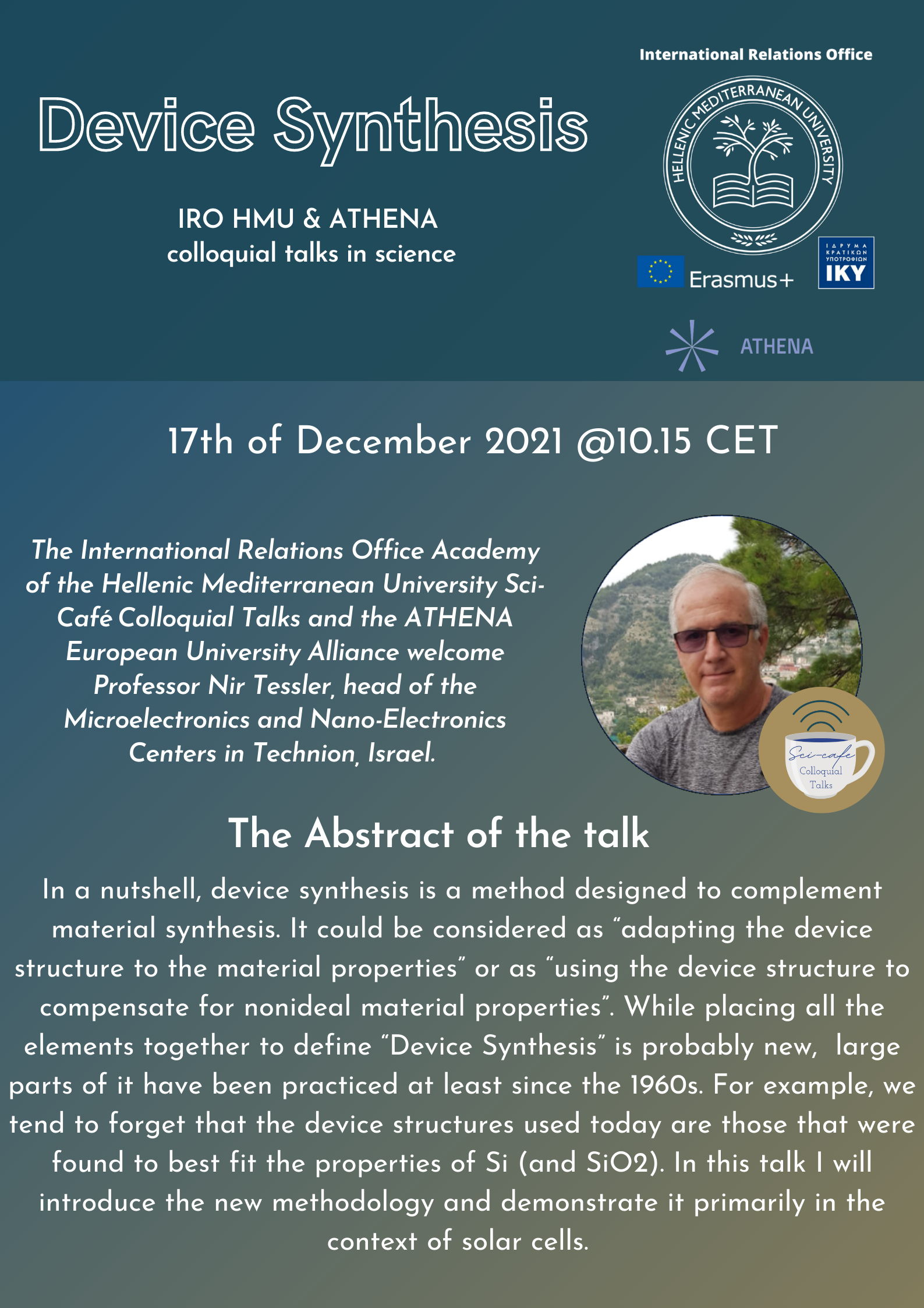
Στα πλαίσια του Sci-Cafe του Γραφείου Διεθνών Σχέσεων, την Παρασκευή αυτή υποδεχόμαστε τον Καθηγητή Nir Tessler απο το Technion στο Ισραήλ. Ο Καθηγητής Nir Tessler είναι από τους πλέον διακεκριμμένους επιστήμονες στον τομέα των εύκαμπτων ηλεκτρονικών και φωτονικών συσκευών. Μαθητής του Sir Richard Friend στο Cambrdige στα διάσημα εργαστήρια του Cavendish, ήταν ο 1ος επιστήμονας που έδειξει πειραματικά lasing μέσω οργανικών ημιαγωγών. Νομίζω ότι είναι μεγάλη μας τιμή να τον έχουμε κοντά μας έστω και διαδικτυακά.
Μερικά λόγια για τον ομιλητή και την ομιλία του ακολουθούν:
Ημερομηνία: 17/10/2021 στις 11.00 πμ
Nir Tessler has been working on Device Physics since starting his Ph.D. (1991) and on Device Chemical-Physics since starting his Post Doc (11/1995). In his Ph.D., he was the first to provide a comprehensive picture of multiple quantum well InP/InGaAs lasers showing that the QWs structure and layout were limiting the modulation speed and thus the communication rate. Six months into his post-doc, at the Cavendish, he demonstrated the world’s first organic semiconductor laser which provided the general community the first direct proof that organics (or PPV at the time) are high-quality semiconductors. In 2002, his group at the Technion was the first to demonstrate and model the charge density and film morphology (or MW) dependence of the charge transport in organic polymers. Over the years his group has been involved with a better understanding of transistors, solar cells, and photodiodes. Some of the by-products were the invention of the perforated source vertical field-effect transistor and solar cell structures for improved device efficiency. His current interests are more towards the electrochemical side of the device operation including mixed ionic electronic transport and reactions, some of which can be found in perovskite solar cells. Nir Tessler currently serves as the head of the Microelectronics and Nano-Electronics centers at the Technion.
Title of the talk: Device Synthesis
In a nutshell, device synthesis is a method designed to complement material synthesis. It could be considered as “adapting the device structure to the material properties” or as “using the device structure to compensate for nonideal material properties”. While placing all the elements together to define “Device Synthesis” is probably new, large parts of it have been practiced at least since the 1960s. For example, we tend to forget that the device structures used today are those that were found to best fit the properties of Si (and SiO2). In this talk, I will introduce the new methodology and demonstrate it primarily in the context of solar cells.
Λινκ στο Zoom:
https://us02web.zoom.us/j/4039520498?pwd=ZVRzUm16T2gwTENwMlh0NnZ3T2FBUT09 Meeting ID: 403 952 0498 Passcode: 477954

